Google splits its AI chip: the TPU 8t trains, the TPU 8i serves, and Axion handles the rest
At Cloud Next 2026, Google unveiled TPU 8t and TPU 8i, an 8th-generation split that matches Nvidia on agentic inference. Ironwood hit GA the same day.
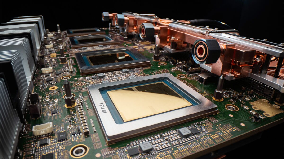
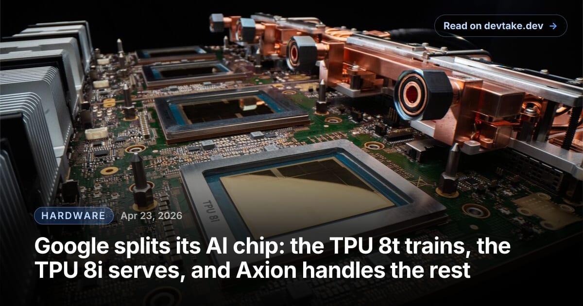
Google used Cloud Next 2026 to break its own TPU pattern. Instead of one next-generation flagship, the 8th-gen TPU is now two chips: the TPU 8t for training and the TPU 8i for inference. Both run on top of Google’s ARM-based Axion CPU host. It’s the first time Google has admitted that one silicon design can’t be the best answer for every phase of an AI workload.
What the split actually buys
The headline numbers Google is pitching: 3x faster AI model training and 80% better performance-per-dollar on inference, both measured against the 7th-gen Ironwood. A single TPU 8t superpod scales to 9,600 chips and delivers roughly 121 exaflops of FP4 compute with two petabytes of shared HBM, according to The Register’s reporting. The 8i triples the on-chip SRAM to 384 megabytes, the memory that matters most when you’re serving low-latency agent traffic and can’t afford to spill to HBM on every KV-cache lookup.
Splitting the roadmap has a real cost. Training chips want enormous HBM and crazy interconnect; inference chips want lots of cheap SRAM, tight batch sizes, and host CPUs that can feed them tokens fast. Trying to hit both on one die means both halves lose. Nvidia has been on the same path with Grace Blackwell’s asymmetric config, and AMD’s MI350 roadmap hinted at it. Google just shipped it first as two distinct SKUs.
The Axion angle matters more than the press release sells it. When the host CPU and the accelerator are both your silicon, you can tune the whole data-path (NUMA, PCIe bandwidth, memory prefetch) without waiting for a third-party vendor’s next socket. Meta bought its way into that world with Broadcom. Google built it in-house.
It’s also a different engineering culture. Nvidia’s strength is the uniformity of its SM design and the CUDA stack that sits on top. You write once, you scale from a laptop 4060 up to a Rubin superpod. Google’s new split assumes the opposite, that training clusters and inference fleets are actually different products run by different teams, and they deserve chips tuned to their own profile. For cloud customers who don’t care about owning the stack end to end, that trade is neutral. For Google, owning the whole stack is the whole point.
Ironwood goes GA, and Anthropic goes huge
Buried under the 8th-gen news is that Ironwood (7th gen) hit general availability on the same day. The Google Cloud post confirms Ironwood superpods hit 9,216 chips, 1.77 PB of shared HBM, and 9.6 Tb/s inter-chip interconnect. The customer quote that’s going to get the most attention is Anthropic’s. James Bradbury, Anthropic’s head of compute, said Ironwood’s scaling will help them run efficiently at their planned footprint: “up to 1 million TPUs.”
That line lands in a specific context. Two days earlier, Amazon announced another $5B into Anthropic and a $100B+ commitment from Anthropic to AWS over 10 years. Anthropic now has multi-cloud compute commitments big enough that it can credibly tell Google and Amazon it’s a serious buyer at both. That’s how you extract good pricing from cloud silicon vendors, and it’s how you avoid being locked into one supply chain when the next chip crunch hits.
Anthropic’s compute story is worth pausing on. A year ago, “1 million TPUs” was the kind of number you saw in research papers about hypothetical future clusters. Now it’s a customer target on a production roadmap. For reference, a million Ironwood chips at 9,216 per superpod is about 108 superpods worth of fabric. Google’s whole AI Hypercomputer pitch is that those superpods can lattice together into one logical cluster, so Anthropic isn’t buying 108 disconnected batches. It’s buying one machine.
Why the inference chip is the real news
For years, TPU coverage has treated training as the main event because that’s where the biggest numbers live. Agentic workloads have flipped the math. If an agent makes 40 LLM calls to finish a task (a plausible shape for Claude Code or ChatGPT’s new workspace agents), then inference is dominant in both cost and latency.
That’s the bet behind the 8i. Triple the SRAM. Better perf-per-dollar on the kinds of workloads that batch poorly and need tight tail latency. And run it all on Axion so Google can keep tuning the host side without depending on Intel or AMD cadence.
Google isn’t claiming it beats Nvidia on every metric. What it is claiming is that when your workload is serving agents, and you want a million-chip cluster under one fabric, Axion + TPU 8i is the cheapest way there. Nvidia’s Vera Rubin is due later this year. The comparison will get sharper once both are shipping.
And the memory shape matters. Inference workloads are famously sensitive to KV-cache residency. Every byte that spills from SRAM into HBM costs you two orders of magnitude in latency. Agentic traffic compounds the problem: longer contexts, more tool calls, more parallel sessions per user. 384MB of SRAM per TPU 8i is a direct answer to that pain. It’s also, not coincidentally, the kind of trade-off Nvidia made on the H200 refresh, and the kind Google used to skip because its TPU v5 and Trillium designs were optimized against a training-dominated world.
That world changed some time in late 2025, and this is the chip that reflects it. If you’re running a production model today, the chips you trained on last year are not the chips that make sense to serve on. Two years ago that was a thesis. Now it’s Google’s product.
What this means for you
If you run models on Google Cloud today: expect Ironwood pricing to soften once 8i lands in preview, because Google needs to move Ironwood capacity. Anthropic’s buildout will eat most of the GA supply, so reserved capacity is about to matter more than on-demand.
If you’re evaluating accelerators: the 3x-training and 80%-inference-per-dollar numbers are Google’s own, so wait for MLPerf. What’s real without waiting is the architectural bet, one chip can’t win both phases, and that’s going to push every other silicon vendor to either split their roadmap or justify why they didn’t.
If you’re on Nvidia and not looking to switch: watch what happens to Vera Rubin’s announced list prices in the next two quarters. Nvidia has room to trim margin before Google’s split starts flipping anchor customers. The shape of that price curve is the most honest signal of whether Google’s pitch actually has teeth.
And if you’re building something smaller than a frontier model (a RAG app, an agent that does some light reasoning and a lot of tool calls), the architectural lesson applies even if the brand names don’t. The chip that trains your model well is almost never the chip that serves it cheapest. Google just made that split explicit. Most shops that operate at scale have already learned it the hard way by paying for training-class silicon to run inference workloads. The less painful version is to right-size your serving hardware for serving and let training happen on a separate fleet.
What about Google’s other Cloud Next announcements
Cloud Next is always a firehose. Alongside the TPU 8 news, Google also added N4A general-purpose Axion VMs (up to 64 vCPUs, 512 GB DDR5, 50 Gbps networking) and C4A compute-optimized ones (up to 72 vCPUs, 576 GB, 100 Gbps, 6 TB local SSD). Vimeo said N4A gave it a 30% transcoding boost, ZoomInfo reported roughly 60% better price-performance, and Rise cut compute 20% on existing C4A workloads. Those aren’t AI-specific numbers, but they’re the grease that makes the AI story go: if your host CPU floor is cheaper and faster, your end-to-end inference cost drops even if the accelerator is the same.
It’s easy to read all of this as another tit-for-tat moment in the accelerator wars. The more honest framing is that Google just told the market its next three years of TPU roadmap won’t look like one flagship chip with a weaker sibling. It’ll look like two chips with two different shapes, tuned for two different realities of how AI actually gets used. Anyone still selling one die for both is now the one who needs to explain why.
Share this article
Sources
- Our eighth generation TPUs: two chips for the agentic era — Google
- Google Cloud launches two new AI chips to compete with Nvidia — TechCrunch
- Google dual tracks TPU 8 to conquer training and inference — The Register
- Ironwood TPUs and new Axion-based VMs for your AI workloads — Google Cloud Blog