IBM's 'sub-1nm' chip is a lab milestone, not a product you'll buy soon
IBM showed a 0.7nm 'nanostack' transistor with ~100 billion transistors on a fingernail. It's real research, but the name is marketing and shipping silicon is years out.
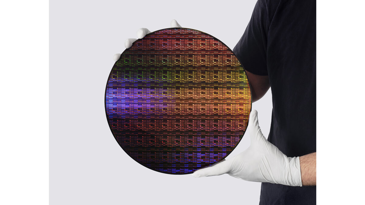
IBM says it built the world’s first “sub-1-nanometer” chip technology. The number is a label, not a ruler reading, and the gap between the two is the whole story. Nothing on the chip is 0.7 nanometers wide, and nothing using it will ship for years, but the engineering underneath is real and worth understanding.
On June 25, IBM debuted what it calls a 0.7nm, or 7-angstrom, transistor architecture named nanostack. The pitch is dense: roughly 100 billion transistors on a chip the size of a fingernail, about twice the density of the 2nm chip IBM showed off in 2021, with up to 50% more performance or up to 70% better energy efficiency at the same node. Those are research numbers from a lab, though. No phone, no laptop, no data-center accelerator ships with this any time soon, and the “0.7nm” name describes none of the physical sizes you’d assume it does.
What IBM actually showed
The real work is a stacking trick, not a shrink. Nanostack takes the gate-all-around (GAA) nanosheet transistors already used at 2nm-class nodes and stacks separate layers of them vertically, staggered, bonded together with what IBM calls 3D sequential integration. That layering is where the density doubling comes from. IBM also says each stacked layer can use different material combinations, so the top and bottom transistors get tuned independently.
This is validated research, with receipts. IBM reports it confirmed ultra-thin dielectric bonding, dual-channel engineering, and a working CMOS inverter switching as expected, which together show the structure can be physically built and actually computes. The development happened at IBM’s Albany NanoTech complex, with tool partners including ASML, Lam Research, Tokyo Electron, and SCREEN.
“With our new nanostack architecture, we’re not just making smaller transistors, we’re reinventing how chips are built to deliver dramatically more power and energy efficiency,” Jay Gambetta, director of IBM Research, said in remarks reported by Reuters. Read it carefully. He says reinventing how chips are built, not shrinking them. That’s the honest version of the headline, and it points straight at how a process node gets named.
Why ‘sub-1nm’ is mostly marketing
Node names stopped mapping to real dimensions years ago. The “0.7nm” figure is a marketing tier, the next rung past 2nm, not the width of anything on the die. As University of Illinois professor Qing Cao put it to MIT Technology Review, “The distance between transistors has been staying at about 40 nanometers for quite a long period of time.” So the gap between transistors is roughly 57 times the node’s name. The number sells. The geometry barely moves.
It helps to see where this sits versus the foundries that actually build chips. TSMC’s A16 angstrom-class node is targeting mass production in 2026, and Intel’s 14A is aiming for a similar window, both leaning on backside power and High-NA EUV. Samsung’s competing 1.4nm-class plan has reportedly slipped. IBM isn’t on that list because IBM doesn’t run high-volume fabs. It develops process technology and licenses it, as it has done before with Samsung and Japan’s Rapidus. We’ve tracked the same scaling pressure from the demand side too, where memory makers reroute output to AI parts and the foundry race reshapes who supplies whom.
What we don’t know yet
The hard parts are the ones IBM hasn’t shown. Yield is the obvious one: stack two transistor layers and a defect in either kills the whole device. “If either top layer or bottom layer fail, your entire chip is going to fail,” MIT Technology Review noted of the approach. Heat is the other. Bonding a second active layer on top means processing it under about 400 degrees Celsius so the lower layer survives, and IBM says it solved that but stayed quiet on how.
Then there’s the calendar. IBM puts production “around five years away,” which in this industry is a soft target, not a ship date. No manufacturing partner has been named for nanostack specifically. Cost is unaddressed, and at these nodes the High-NA EUV tooling runs into the hundreds of millions of dollars per scanner. The competitive picture is crowded, too. Intel, Samsung, TSMC, and the imec research hub are all chasing similar stacked-transistor (CFET) ideas, so “first” here means first to publish this particular variant, not first to a market.
Sourcing: the figures and the architecture come from IBM’s own newsroom release, and Reuters and MIT Technology Review corroborated them and supplied the skeptical context. Full links sit in the sources list below.
What this means for you
If you build software, buy hardware, or just read chip headlines, treat “sub-1nm” as a research banner, not a spec you’ll see on a product page in 2027. The useful signal here is direction: scaling has shifted from making transistors smaller to stacking them in three dimensions, and that’s where the real engineering fight now lives. For anyone shopping AI accelerators or planning capacity, the names that matter near term are TSMC’s A16 and Intel’s 14A, the nodes actually entering production, not IBM’s lab demo. The honest read on nanostack: it’s a credible bet that Moore’s Law has another decade in it, with the catch that “another decade” means roughly five more years before this specific idea even tries to ship. Watch which foundry licenses it. That’s the moment it stops being a press release.
Share this article
Quick reference
- process node
- A chipmaker's name for a generation of its manufacturing process, like 2nm or 0.7nm. The number is a marketing label now, not a real measured dimension on the chip.
- nanostack
- IBM's name for vertically stacking and staggering transistors in separate layers, joined by 3D sequential integration, to raise density without shrinking the transistors.